Handset E1
A from-scratch Android phone design: generated KiCad schematics, parametric frame CAD and a gated release workflow.
- Status
- Designed, unbuilt
- Period
- Nov 2026
- Discipline
- Hardware
- Reference
- KL-M1
Overview
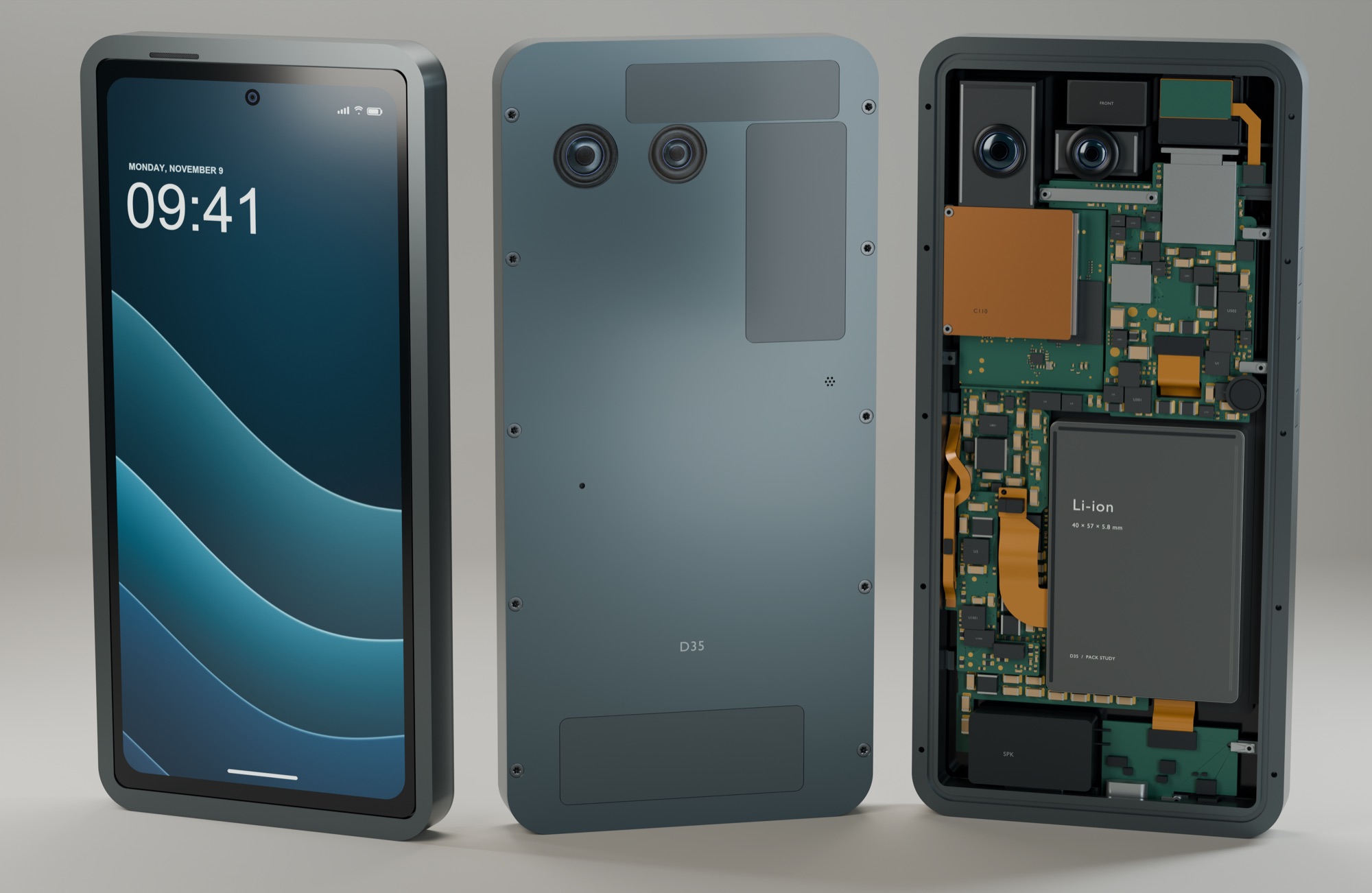
This is my attempt to design a complete Android phone: main board, bottom flex, machined aluminium frame, printed back panels and bring-up software. The first four days produced revisions D1 to D43, a 163.4 x 78.0 x 10.5 mm handset built around a compute module with a separate radio board, a vapour chamber and a copper bridge. Each subsystem had its own KiCad project and the assembly lived in Blender with about 495 selectable CAD placements. The upper boards were never fully routed. On 10 November 2026 I abandoned that line and restarted as E1.
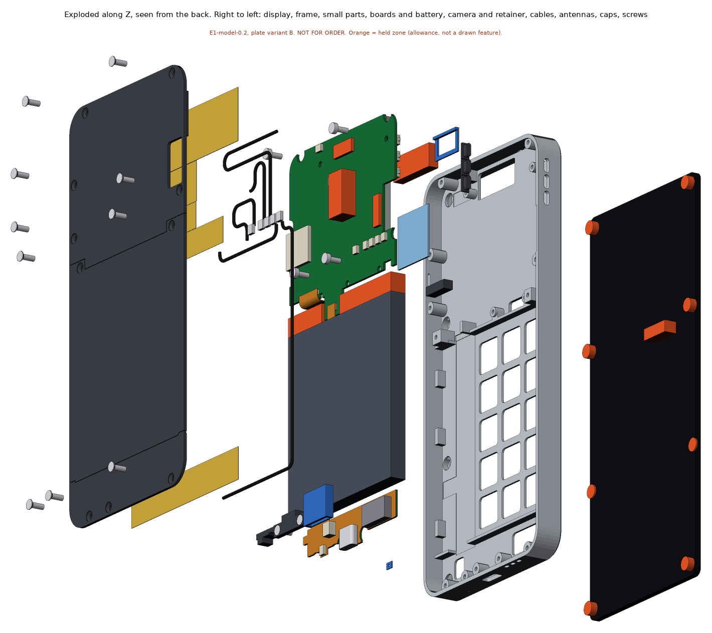
E1 is a clean-sheet design with screws-only assembly. One rigid main board sits in the top 59 mm behind the display. A small flex in the bottom band carries the USB-C socket, a microphone and speaker contacts, and its tail crosses the battery to plug into the main board by hand. The compute and radio are one part, an off-the-shelf smart module. The display, cameras and battery are spare parts sold for a repairable production phone, and the battery sits behind a printed door held by two screws.
The rule that shapes everything is that nothing can be bought first to measure. Every pin map, dimension and rating has to come from published manufacturer data, or the design has to tolerate the whole published range. Where data is missing, the part is drawn as a keep-out box and not guessed. The display socket and two camera sockets are held this way. Battery polarity is unproven, so a P-channel FET in the positive lead blocks a reversed pack while USB is unplugged, and the procedure adds a bleed-and-measure step before every plug-in.
The schematic is not drawn by hand. An architecture file describes each board, rail and connection, and a Python generator turns the circuit data into KiCad sheets. The output is checked with KiCad 10 ERC, a netlist compare against the source data, and a 21-point merge check. The 636-land module footprint was rebuilt from the vendor's vector drawing and audited separately. The frame is parametric CAD with STEP output, a feasibility model for outline, thickness, mass and first-order heat, and exploded views. Most of this was produced by coding agents working to my requirements and review.
E1 has a schematic and a mechanical model, and no PCB layout. Every stage of the release workflow, from product definition through sourcing and circuit, is marked blocked. The open items are the unidentified sockets, the battery polarity, Android source for the module, and several deviations from the brief that I have not yet accepted, including 4 GB of memory where the brief asks for 8 GB.
Specifications
- Schematic revision E1-sch-0.4: main board 271 parts, 212 nets and 12 pages; bottom flex 21 parts, 20 nets and 3 pages.
- KiCad 10.0.6 ERC reports 0 errors and 0 warnings on both boards, the netlist compare is exact, and merge checks C1 to C21 pass.
- Main board specification: rigid, 8 layers, 1.0 mm, HDI with copper-filled laser vias, controlled impedance at 85 ohm for display and camera pairs, 90 ohm for USB and 50 ohm for antenna feeds.
- Design limits are an outline no larger than 163.4 x 78.0 mm, at most 220 g and about 12 mm thick; the feasibility model gives a 160.0 x 76.2 mm outline and an 11.23 mm stack over the battery.
- The battery is a 4415 mAh typical pack charged to 4.40 V, with a modelled 0 to 50 percent charge in about 41 minutes if the charger supplies 3 A throughout.
- The always-on system rail is budgeted at 1.43 A peak against a 1.5 A limit, with the display bias behind a current-limited switch set to at most 0.789 A.
- The sourcing lock lists 70 rows covering 290 references.
- The earlier D-series reached revision D43 in four days, with a Blender assembly of about 495 CAD placements across 19 views.